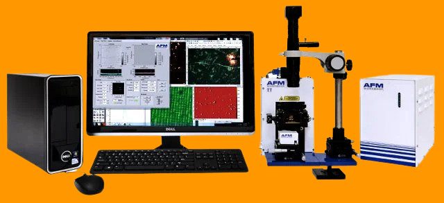
An atomic force microscope (AFM) is a versatile high-resolution scanning probe microscope that is used very much for analyzing samples in great detail. The image can be magnified over a hundred million times by this microscope. Angstrom scale is used to scan the samples. It can create 3D structures rather than 2D structures to uncover hidden information.
The resolution of this microscope is generally identified at a nanometer level, which is much more effective and accurate than the optical diffraction limit. A probe is used by this microscope to measure and collect the data involves touching the surface that has the probe. The three-dimensional structure of the sample is formed when the scanning probe microscope raster-scans the probe over a section of the sample. This atomic force microscope was invented in 1982 and it was first used experimentally in 1986.

The Principle of AFM
The principle of the Atomic Force Microscope relates to the surface sensing technique by using an extremely sharp tip on a micromachined silicon probe. This sharp nano-scale tip is attached to a small cantilever which forms a spring. The bending is detected by using a laser diode and a split photodetector after contacting the tip on the surface and the cantilever bends.
Dynamic and contact modes are used as the operating mode of this microscope. The tip is pressed into the surface in contacting mode and an electronic feedback loop monitors the tip-sample interaction force for keeping the deflection constant throughout raster scanning. Tapping mode fixes the contact between the surface of the sample and the tip to protect both from any kind of damage.
It is possible easily for the vibrating of the cantilever near its resonance frequency in this tapping mode. The tip can move up and down in what is described as a sinusoidal motion. But this motion can be reduced by attractive or repulsive interactions as it comes near the sample. A feedback loop is also used in a similar way to contact mode, except it helps to keep the level of amplitude of tapping motion constant rather than the level of quasistatic deflection. Finally, the sample topography can be traced easily line by line after completing these steps.
Instrumentations of Atomic Force Microscope
AFM microscope is one kind of versatile tool which is used for topographical measurements and imaging applications. It helps to identify mechanical and electrical material properties, alongside ferro- and piezoelectric, thermal, and magnetic properties.
The probe tip of this microscope is important to characterize the electromechanical coupling of a material system using electrical stimulation. But it requires high tip-bias voltages for achieving suitable levels of sensitivity. Contact mode is also very important for measuring the electrical properties of samples during imaging. This microscope has different following parts that are very essential in controlling its functions.
Modified tips: These tips are used for detecting the sample surface and undergoing deflections.
Software adjustments: These are important for creating images of the samples.
Feedback loop control: The force interactions and the tip positions can be controlled by this system using a laser deflector. The tip interacts with the surface of the sample after reflecting the laser from the back of the cantilever and the tip. The laser’s position on the photodetector helps in tracking the surface of the sample and measurement.
Deflection – The Atomic Force Microscope device consists of a laser beam deflection system. The laser system of this device reflects from the back of the AFM lever to the sensitive detector. Silicon compounds with a tip radius of about 10nm are used for constructing these.
Force measurement – The works of an Atomic Force Microscope highly depend on the force interactions which contribute to the production of the image. It can be measured the forces by calculation of the deflection lever after knowing the stiffness of the cantilever.
Applications of Atomic Force Microscope (AFM)
Atomic Force Microscope has been used for imaging and conducting a deep analysis of samples. It is possible to study surface textures, defects, coatings, and tons of other physical features of various samples by helping this instrument. This technology is very suitable for observing cells and biomolecules in their natural environment. Microelectronics circuits and components can be analyzed by this instrument. Batteries and energy generation materials properties can also be investigated by applying this technology.
This modern device is very much used in various disciplines such as solid-state physics, molecular engineering, polymer chemistry, semiconductor studies, surface chemistry, molecular biology, cell biology, medicine, physics, and other prominent fields for observation and research. It helps to identify atoms from samples. It evaluates force interactions between atoms. It helps to detect various physical changing properties of atoms. The structural and mechanical properties of protein complexes and assembly can be evaluated by helping this instrument.
The shape of the cell and its wall rigidity can be identified by this modern device. The main drawbacks of the AFM are that it has low scanning speed and the inability for evaluating the chemical properties of the surface under observation.
References
Binnig, G., Quate, C. F., & Gerber, C. (1986). Atomic force microscope. Physical review letters, 56(9), 930.

